Crazy! ece rocks: vlsi layout designs Analog vlsi design Vlsi design: vlsi tutorial (vlsi design
VLSI layout view of the LDPC decoder | Download Scientific Diagram
Vlsi layout mux Chip observing boom transistors Stick-diagrams (2) vlsi
Vlsi analog example short description
Vlsi design: vlsi tutorial (vlsi designVlsi_diagrams_02.jpg — are.na What is the function of stick diagram in integrated circuit layout designPhysical layout design example..
What is physical design in vlsiVlsi circuit design Vlsi cadence final virtuoso crc using res hi version large clickVlsi layout design methods layout design steps partitioning.

Ee5323 vlsi design i using cadence
Design vlsi layout and schematic on cadence by ex_einstien_palLayout cadence inverter virtuoso vlsi inv cell create tutorial ece umn edu How to draw vlsi stick diagrams ?Vlsi design flow.pptx.
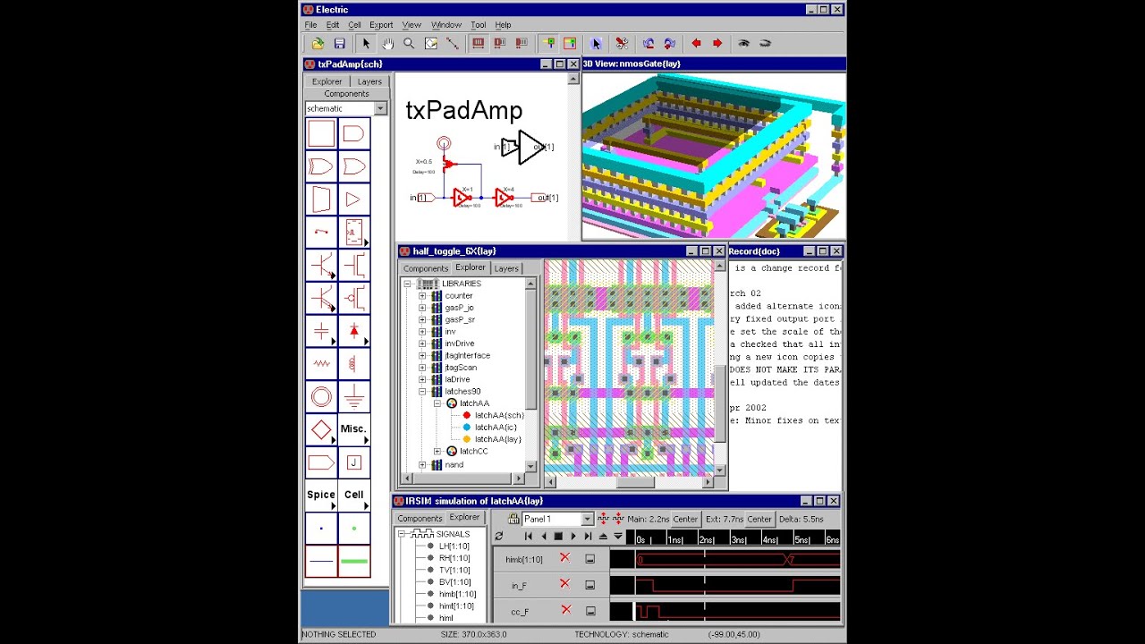
Vlsi cadence layout schematic full fiverr screenVlsi concepts: november 2014 Electric vlsi tutorialWhat is layout design in vlsi.
The block diagram of the vlsi architecture of the fft-based mimo
Vlsi lab layoutsFigure 1 from schematic driven layout for the custom vlsi design Figure 2 from schematic driven layout for the custom vlsi designPpt lecture 10: circuit families powerpoint presentation,, 51% off.
Vlsi layout view of the ldpc decoderVlsi design: layout of static cmos circuits Stick vlsi diagram layout circuit integrated system functionArt of layout – euler’s path and stick diagram – part 1 – vlsi system.

Solved answer the following two questions related to vlsi
(ppt) vlsi design circuits & layoutGrant h. Steps in the vlsi circuit design flow [86]Vlsi_diagrams_12.jpg — are.na.
Vlsi design: vlsi tutorial (vlsi designVlsi layout Diagram stick layout path euler vlsi part'network-on-a-chip' : a note on its genesis.


Figure 1 from Schematic driven layout for the custom VLSI design

VLSI LAB layouts - Vlsi lab - Electronic and communication - VLSI LAB

Design vlsi layout and schematic on cadence by Ex_einstien_pal | Fiverr

What Is Layout Design In Vlsi - Design Talk

Figure 2 from Schematic driven layout for the custom VLSI design

VLSI layout view of the LDPC decoder | Download Scientific Diagram

VLSI_diagrams_02.jpg — Are.na
![Steps in the VLSI Circuit Design Flow [86] | Download Scientific Diagram](https://i2.wp.com/www.researchgate.net/publication/363889257/figure/fig1/AS:11431281086771580@1664335251480/Steps-in-the-VLSI-Circuit-Design-Flow-86.jpg)
Steps in the VLSI Circuit Design Flow [86] | Download Scientific Diagram